■Overview
< MM3456 >, Mitsumi has developed a device capable of high-efficiency charging, including a DMOS FET with low on-resistance and 40V withstand voltage.
A maximum peak current of 2.0 A on the primary side of the transformer means that the flash capacitor can be charged at high speed.
We have also developed a small, highly reliable step-up transformer for the flash, and can offer the flash and transformer as a pair with matched characteristics.
§ Features
1. |
Realizes high-efficiency charging thanks to built-in switching DMOS FET with 40 V withstand voltage and low on-resistance. |
2. |
Enables construction with reduced number of components thanks to detection of charging completion on primary side of transformer. |
3. |
Primary side peak current can be set to a maximum of 2.0 A (3 steps, 2 ranks) for high-speed charging of flash capacitor. |
4. |
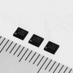
Small package size (2.5 × 2.7 × 0.6 mm max.) |
§ Main specifications
 |
|
 |
SW terminal peak current |
1.0, 1.2, 1.4 A (1.6, 1.8, 2.0) 3 steps, 2 ranks |
|
VCC current consumption |
1.3 mA max. |
|
Zero current detection voltage |
50 mV (Vsw-VBAT) |
|
Charging completion detection voltage 1 |
22 V ± 1% (Ta = 25ºC) |
|
Charging completion detection voltage 2 |
1.2 V ± 1% (Ta = 25ºC) |
|
Maximum on-time |
100 usec. |
|
Package |
SSON-10 |
|
Dimensions |
2.5 × 2.7 × 0.6 max. (Unit: mm) |
|
 |
 |